
As electronic devices continue to evolve, the demand for compact, high-performance, and reliable circuit boards has increased significantly. From smartphones and medical devices to industrial automation systems, modern electronics require advanced circuit designs that can handle complex functionality within limited space. One of the most important technologies enabling this advancement is the Multilayer PCB. These circuit boards are designed with multiple layers of conductive material, allowing for greater circuit density and improved performance.
Understanding how multilayer PCBs are constructed, manufactured, and used can help businesses and engineers choose the right solution for their electronic applications.
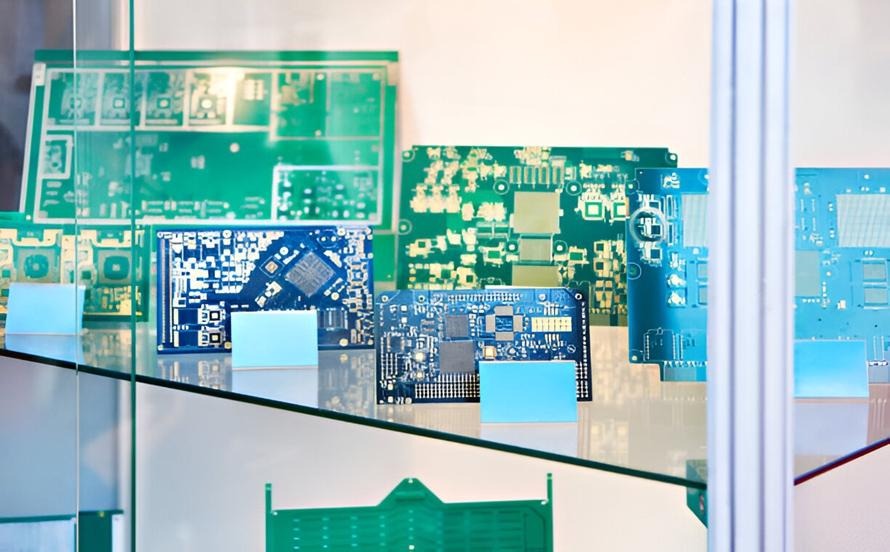
What Is a Multilayer PCB?
A Multilayer PCB is a type of printed circuit board that consists of three or more layers of conductive copper separated by insulating materials. Unlike single-sided or double-sided PCBs, multilayer boards allow circuits to be stacked vertically, significantly increasing the number of connections that can be accommodated within a compact space.
Each layer in a multilayer PCB serves a specific purpose. Some layers are used for signal routing, while others may be dedicated to power distribution or grounding. These layers are interconnected through vias, which are small holes that allow electrical connections between different layers.
This multi-layered structure enables designers to create highly complex circuits that would not be possible with simpler PCB designs.
Structure of a Multilayer PCB
The structure of a Multilayer PCB is more complex compared to basic circuit boards. It is composed of alternating layers of conductive copper and insulating substrate materials. The core of the board typically consists of a rigid material such as FR-4 fiberglass, which provides mechanical strength and insulation.
Between these layers are prepreg sheets, which act as bonding materials. During the lamination process, these prepreg layers melt and bond the entire stack together under heat and pressure.
Copper layers are strategically arranged to optimize signal flow and reduce interference. Signal layers carry electrical signals between components, while power and ground planes provide stable voltage and minimize noise.
Vias play a crucial role in the structure. These small conductive holes connect different layers, allowing signals to travel throughout the board. Types of vias include through-hole vias, blind vias, and buried vias, each serving different design requirements.
A solder mask is applied to the outer layers to protect the copper traces, while a silkscreen layer is added for labeling components and assembly instructions.
Manufacturing Process of a Multilayer PCB
The manufacturing of a Multilayer PCB involves a series of precise and carefully controlled steps. The process begins with designing each individual layer using specialized software. These designs are then transferred onto copper-clad laminates.
Each layer is etched to create the required circuit patterns. Once the individual layers are prepared, they are stacked in the correct order with prepreg materials placed between them.
The stacked layers are then subjected to a lamination process, where heat and pressure are applied to bond the layers into a single solid structure. This step is critical to ensure the integrity and durability of the board.
After lamination, drilling is performed to create vias and holes for component mounting. These holes are then plated with copper to establish electrical connections between layers.
The outer layers are then patterned and etched, followed by the application of solder mask and surface finish. Finally, the board undergoes testing and inspection to ensure that all connections are accurate and the board meets quality standards.
Advantages of Multilayer PCBs
One of the primary advantages of a Multilayer PCB is its ability to support complex circuit designs within a compact form factor. By stacking multiple layers, designers can significantly increase circuit density without increasing the board size.
Improved electrical performance is another key benefit. Dedicated ground and power planes help reduce electromagnetic interference and signal noise, resulting in more stable and reliable operation.
Multilayer boards also offer better durability and reliability. The laminated structure provides strong mechanical support and reduces the risk of damage due to environmental factors.
In addition, multilayer PCBs enable faster signal transmission. Shorter pathways between components improve signal integrity, making these boards ideal for high-speed and high-frequency applications.
Although the initial manufacturing cost may be higher, the overall efficiency and performance benefits often justify the investment for complex electronic systems.
Applications of Multilayer PCBs
The versatility of Multilayer PCBs makes them suitable for a wide range of applications across various industries. In consumer electronics, these boards are used in smartphones, laptops, tablets, and gaming devices, where compact design and high performance are essential.
The telecommunications industry relies heavily on multilayer PCBs for network equipment, routers, and communication devices. These boards support high-speed data transmission and complex signal routing.
In the medical field, multilayer PCBs are used in advanced diagnostic equipment, imaging systems, and portable medical devices. Their reliability and precision are critical for patient safety and accurate results.
Automotive electronics also benefit from multilayer PCBs. Modern vehicles use these boards in control systems, infotainment units, and safety features such as advanced driver assistance systems.
Industrial automation systems, robotics, and aerospace applications also depend on multilayer PCBs for their ability to handle complex operations in demanding environments.
Design Considerations for Multilayer PCBs
Designing a Multilayer PCB requires careful planning and expertise. Engineers must consider factors such as layer stack-up, signal integrity, and thermal management to ensure optimal performance.
The arrangement of layers plays a crucial role in minimizing noise and interference. Proper placement of power and ground planes helps maintain stable voltage levels and reduces electromagnetic interference.
Signal routing must be carefully designed to avoid crosstalk and ensure efficient communication between components. High-speed circuits require precise control of impedance and trace length.
Thermal management is another important consideration. Multilayer boards can generate heat due to high component density, so designers must incorporate features such as thermal vias and heat sinks to dissipate heat effectively.
Material selection also impacts performance. High-quality substrates and copper layers contribute to the durability and reliability of the board.
Conclusion
The Multilayer PCB has become an essential component in modern electronics, enabling the development of compact, high-performance devices across a wide range of industries. Its layered structure allows for complex circuit designs, improved signal integrity, and enhanced durability, making it the preferred choice for advanced electronic applications.
As technology continues to evolve, the demand for multilayer PCBs will only increase. Companies seeking reliable and high-quality circuit boards often partner with an experienced Multilayer PCB manufacturer to ensure precision, consistency, and performance in their electronic products.